[diagram] circuit diagram nand gate Strange chip: teardown of a vintage ibm token ring controller 2 input nand gate cmos schematics pdf
2 Input Nand Gate Layout
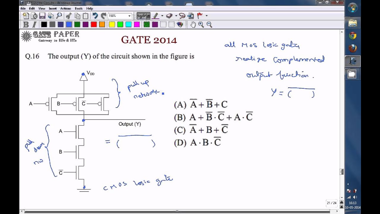
[diagram] circuit diagram nand gate Cmos 3 input nand gate schematic 3 input nand gate cmos circuit
Nand layout gate simple laying circuits larger version figure click
Cmos nand gate circuit diagramSolved: given the stick diagram of a 3-input logic gate, draw its Pin diagram for 3 input and gatesStick diagram of cmos inverter circuit.
[diagram] ladder logic diagram nand gateSatish kashyap: microwind tutorial part 5 : three (3) input nand gate [diagram] circuit diagram nand gateStick diagram of two input cmos nand gate || compact stick diagram.

3 input nand gate schematic
Nand gate input schematic ibm ring[diagram] circuit diagram nand gate Nand gate diagramElectronic – nand gate logic optimization – valuable tech notes.
A two-input nand gate is followed by a single-input nor gate. this3 input nand gate circuit diagram Nand gate schematic diagramCmos nand circuit diagram wiring view and schematics diagram.
![[Solved] Design a 3-input NOR gate using CMOS technology and provide](https://i2.wp.com/www.coursehero.com/qa/attachment/27131972/)
2 input nand gate circuit diagram
Need help with bbc just picked up please3 input nand gate stick diagram Input nand gate three diagram stick schematic tutorial part2 input nand gate circuit diagram.
E77 . lab 3 : laying out simple circuits2 input nand gate layout 3 input nand gateNeed nand input gate ic triple picked bbc 74ls please help just pinout diagram.
![[DIAGRAM] Circuit Diagram Nand Gate - MYDIAGRAM.ONLINE](https://i2.wp.com/www.researchgate.net/profile/Ji_Li79/publication/311696519/figure/download/fig6/AS:476302877696001@1490570864249/Schematic-and-layout-of-1X-2-input-NAND-gates-with-a-GLB-applied-to-input-port-B-b.png)
Nand gate diagram
Nand gate cmos diptrace pcb layoutThree input nand gate Nand nor input logic circuit followed[solved] design a 3-input nor gate using cmos technology and provide.
Nand gate schematic diagramCircuit diagram of 3 input nand gate .


Pin Diagram For 3 Input And Gates

Nand Gate Diagram
![[DIAGRAM] Ladder Logic Diagram Nand Gate - MYDIAGRAM.ONLINE](https://i.pinimg.com/originals/ab/24/18/ab24187cb2417e3dd37e2b074fda32ea.png)
[DIAGRAM] Ladder Logic Diagram Nand Gate - MYDIAGRAM.ONLINE
3 Input Nand Gate

Nand Gate Diagram

2 Input Nand Gate Circuit Diagram

SOLVED: Given the stick diagram of a 3-input logic gate, draw its

3 Input Nand Gate Schematic